


Data Sheet

  CPU         : 6510 @ 0.9852484444MHz [1] (PAL)
                       1.0227277143MHz [1] (NTSC)
  RAM         : 64kB DRAM
                .5kB SRAM (color RAM $d800-dbff)
  ROM         : 20kB ROM total, consisting of three ROMs
                (BASIC and Kernal share one ROM on new boards):
                  - 8k BASIC V2      ($a000-bfff)
		            - 8k Kernal        ($e000-ffff)
		            - 4k character ROM ($d000-dfff)
  Graphics    : VIC-II ($d000-d3ff)
  Sound       : SID ($d400-d7ff)
  Int. drives : -
  Interfaces  : 2 x control port (CIA #1 ($dc00-dcff)),
				  audio/video,
	              cassette port (CIA #1)
                  expansion port,
                  serial IEC (CIA #2 ($dd00-ddff)),
		          TV,
                user port (CIA #2)
  Keyboard    : 66 keys, controlled by CIA #1
  Power supply: external transformer (9VAC + 5V DC)
  Extras      : We don't need no frills ;-)
![[Picture of original NTSC C64 board]](pics/c64pcbvoNTSC.jpg)
![[Picture of original PAL C64 board]](pics/c64pcbvoPAL.jpg)
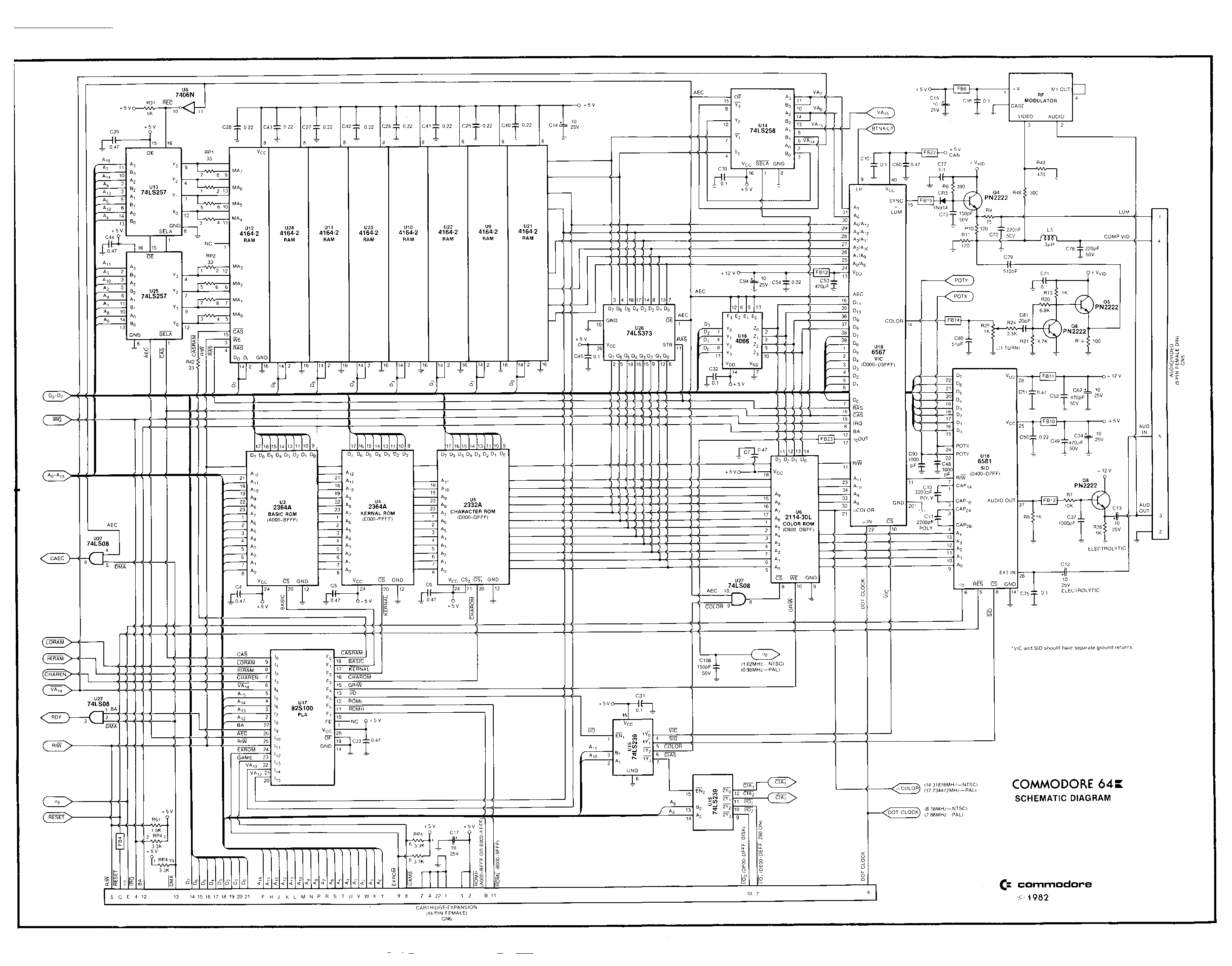
Schematics: 158k
GIF, 2897x2273 (Part 1), 131k
GIF, 2669x2800 (Part 2)
Known revisions: ?
According to [2], this board has the PCB ASSY #326298-01; it can easily be recognized by its 5-pin video jack. The serial reset line is directly connected to the CPU so that you can use a serial reset button to reset the C64 (and all serial devices) [This is an assumption, because this is the case with the succeeding version A].
The following is an enumeration of features that all old boards (including #250441) have in common:
Please see below (Version B) for a discussion on the location of the SID and the PLA, before you start replacing them!
[ Help! Can you verify the
PLA and SID locations? ]
[ Help! Can you verify that the CPU reset is
directly connected to the serial reset? ]
![[Picture of original C64 board]](pics/c64pcbva.jpg)
[ Help! Schematics wanted! ]
Known revisions: REV.A, REV.B, REV.C
This board bears the PCB ASSY #250407 (or PCB ASSY
#250407-04 according to [2]).
It is the first C64 board using an 8-pin video jack, all newer boards use this
connector. You can recognize this particular board by looking through the
expansion port (viewing from behind, it is on the left side). If the rectifier
bridge (it's in a black plastic case of 1x1cm) is BEHIND the fuseholder (which
means that you might not be able to see it), then it's a version A (CR) board,
if it is to the LEFT of the fuseholder, it's a version B board (or newer?).
Please see below (Version
B) for a discussion on the location of the SID and the PLA, before
you start replacing them!
[ Help! What is the difference between version A and CR or ACR? ]
![[Picture of C64 Rev B board]](pics/c64pcbvb.jpg)
Known Revisions: ?
The PCB ASSY #250425 is not the only thing in which this
board differs from the others. First of all, it has a reduced oscillator
circuit; the numerous TTL chips providing both DOT and color clock have been
replaced by a single clock generator IC (MOS 8701). Then the VIC-II's alignment
has been changed from vertical to horizontal, so that pin 1 is in the lower left
corner. Furthermore, the locations of SID (U18) and PLA (U17) have been SWAPPED,
at least with respect to Version A (CR), so that the SID now resides near the
upper edge of the board and the PLA an inch below. So VERY CAREFULLY
check where to put SID and PLA if you want to replace them or swap them with
chips from another board! The SID has to be placed into U18 and the PLA into
U17.
Additionally to changing the color RAM's location (U6), Commodore also changed the location of the rectifier
bridge (CR4), by which you can easily tell this version from version A (CR) (see
Version A above).
In some revisions, the
resistors R29 and R30 have piggybacked diodes, which seem to be protecting two
lines of the serial port [?].
[ Help! What is the revision of the 'piggyback' boards? ]
Known Revisions: ?
I haven't seen this board yet - actually I'm too lazy to open all my C64s to check for this board :-) All I know is that it has the PCB ASSY #250441-01. [2] states:
 All circuits remain the same as the 64B (Schematic 251469)
 with a few component location changes:

    1) Resistors 28, 29, 30, 36, 48 were reduced to Resistor
       Pack RP5.
    2) Diodes CR100-105 are no longer piggybacked. Their new
locations are CR9, 12-16.[ Help! How can you tell this version from prior versions without opening the case? ]
![[Picture of C64 Rev B board]](pics/c64_250466.jpg)
(apologies for the picture, I had to paste it together from two sources)
[ Help! Schematics wanted!
]
Known Revisions: A
Someone donated a C64 with this board on 98/2/13. It has the PCB ASSY
#250466-01. The most obvious difference to the previous boards is
that it is the first board to use two 64kx4 DRAM chips, like in the new boards.
Please see above (Version
B) for a discussion on the location of the SID and the PLA, before
you start replacing them!
Schematics: 235k
GIF, 3453x3009 (this diagram has been corrected quite a lot, but
possibly still has errors. If you find them before we do, mail me!)
Known Revisions: REV.3, REV.4,
REV.B
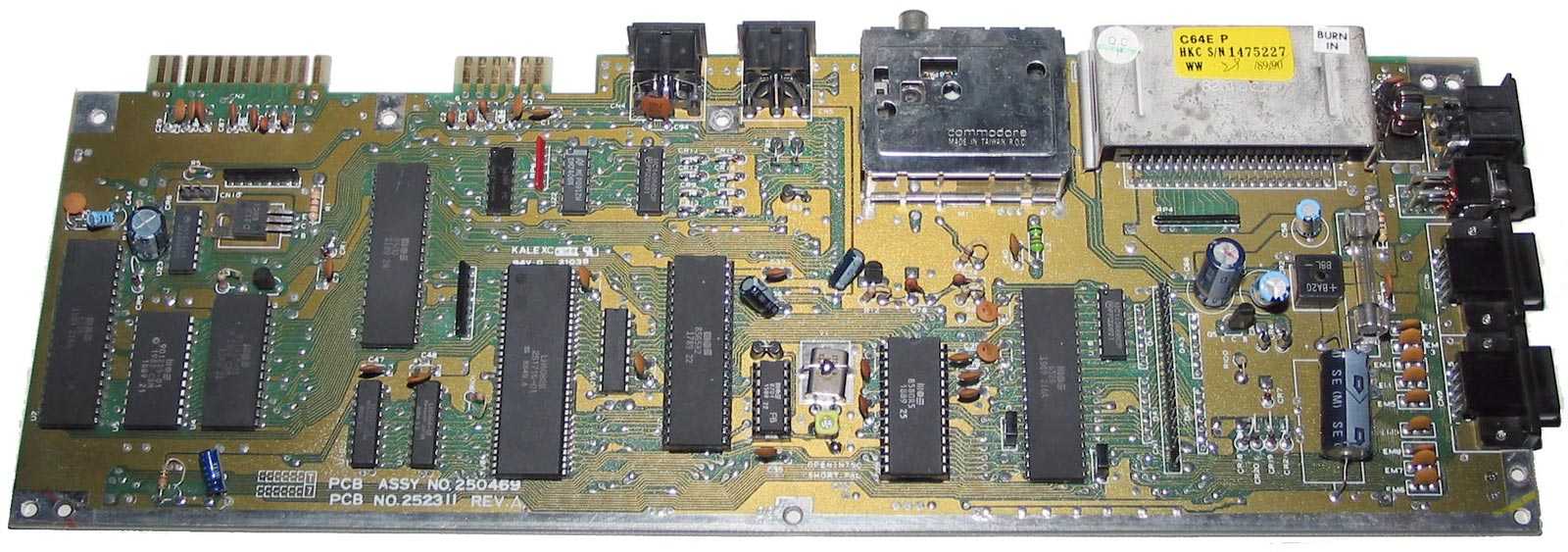
This is the first version of the totally redesigned boards, which were first
employed in the C64G in 1987. It has the PCB ASSY #250469, REV.3
and along with the following boards, it will be referenced as 'short board'. The
64'er stated that this version has no 9VAC at the user port [3]
('ALDI' version, see notes at the end of this section). I have a board of the
same revision and one of REV.4, and both of them do have 9VAC at the user port.
The easiest way to describe this board
is to state that the location of the ports hasn't changed. :-) Ok, let's
enumerate the major changes of this version:
![[Picture of new, short C64 board with color RAM in MMU, 35k JPEG]](pics/c64pcbrb.jpg)

[ Help! Schematics wanted! ]
The main difference of REV.B, which was introduced in the end of 1990 [?], from REV.3/4 is that the color RAM is now in the MMU. This means that if the color RAM is damaged, you would have to exchange the MMU, which is not very easy, since it has a very narrow raster and 64 pins. Additionally, Commodore decided to protect CIA #1 by replacing the capacitors EM1-EM9 with strange looking capacitor/resistor combinations, the capacitors of which are said to break down easily and pull the appropriate input to GND.
Recognizing these new generation boards is easy: Look through the user port; if you can see two big chips sitting next to each other (the two CIAs), it's an old board, otherwise, it's a new, short board.
[ Help! What is the NAME of this version? Version C maybe? ]
| Old boards | New boards | ||||||
|---|---|---|---|---|---|---|---|
| Original | #250407 | #250425 | #250441 | #250466 | #250469R4 | #250469RB | |
| 4066 (paddles) | ? | U28 | ? | U28 | U18 | ||
| 4066 (ColorRAM) | ? | U16 | ? | U16 | U21 | ||
| 556 | ? | U20 | ? | U20 | - | ||
| 7406 | ? | U8 | ? | U8 | U22 | ||
| BASIC ROM | ? | U3 | ? | U3 | U4 (incl. Kernal) | ||
| Character ROM | ? | U5 | ? | U5 | U5 | ||
| CIA #1 ($dc00) | U1 | ? | U1 | ||||
| CIA #2 ($dd00) | U2 | ? | U2 | ||||
| Color RAM | ? | U6 | ? | U6 | U19 | - | |
| CPU | U7 | ? | U7 | U6 | |||
| DRAM | ? | U9-12 U21-24 | ? | U9-U10 | U10-11 | ||
| Kernal ROM | ? | U4 | ? | U4 | U4 (incl. BASIC) | ||
| MMU | - | ? | - | U8 | |||
| PLA | U17 | ? | U17 | - | |||
| SID | U18 | ? | U18 | U9 | |||
| VIC-II | ? | U19 | ? | U19 | U7 | ||
[ Help! Can you fill out the rest? Please VERIFY locations on your board first! ]