ROM Socket Adapters
Socket adapters are required on the original C64 and 1541 models when replacing the existing 24-pin ROM with a 28-pin EPROM, like a 2764 or larger. They are also needed if you want to replace a 2764 with a larger 27128, a 27128 with a 27256 or a 27256 with a 27512. All of these adapters are covered here.
The nice thing about the 2764 through 27512 is they are basically drop-in pin compatible, the only thing extra are more address lines. From the 2764 to the 27128 there is the addition of A13 (address line 13) on pin 26. From the 27128 to the 27256 there is A14 on pin 27 and from the 27256 to the 27512 there is A15 on pin 1. As long as you deal with those address lines by tieing them high through a 4.7K resistor and switching them in/out to bank the EPROM) or simply tie them high to Vcc or low to ground, you will be OK.
Building a 28-24 Pin ROM adapter for 2764 EPROMs for original C64's and 1541's.
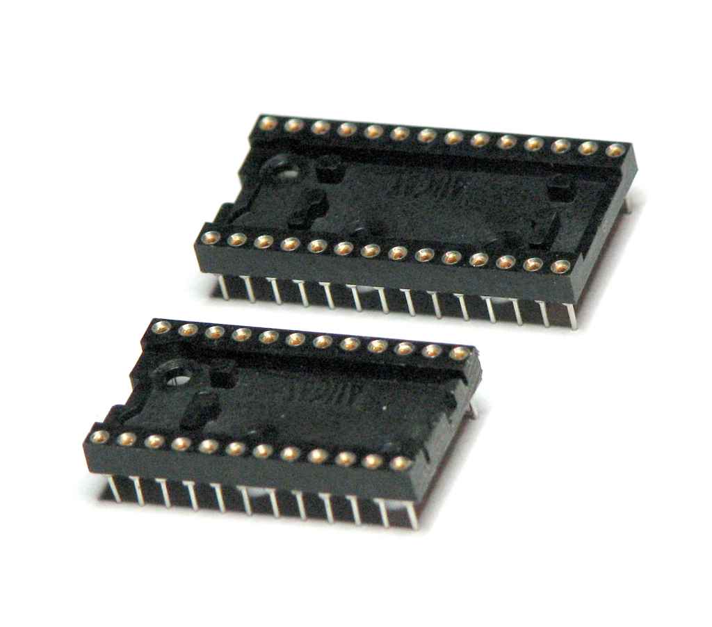 |
Step 1: Obtain a 28 pin and 24 pin precision socket. These have the round pins (not flat) and are more expensive than standard chip sockets. The 28 pin will go on the top and the 24 pin will be on the bottom when completed. |
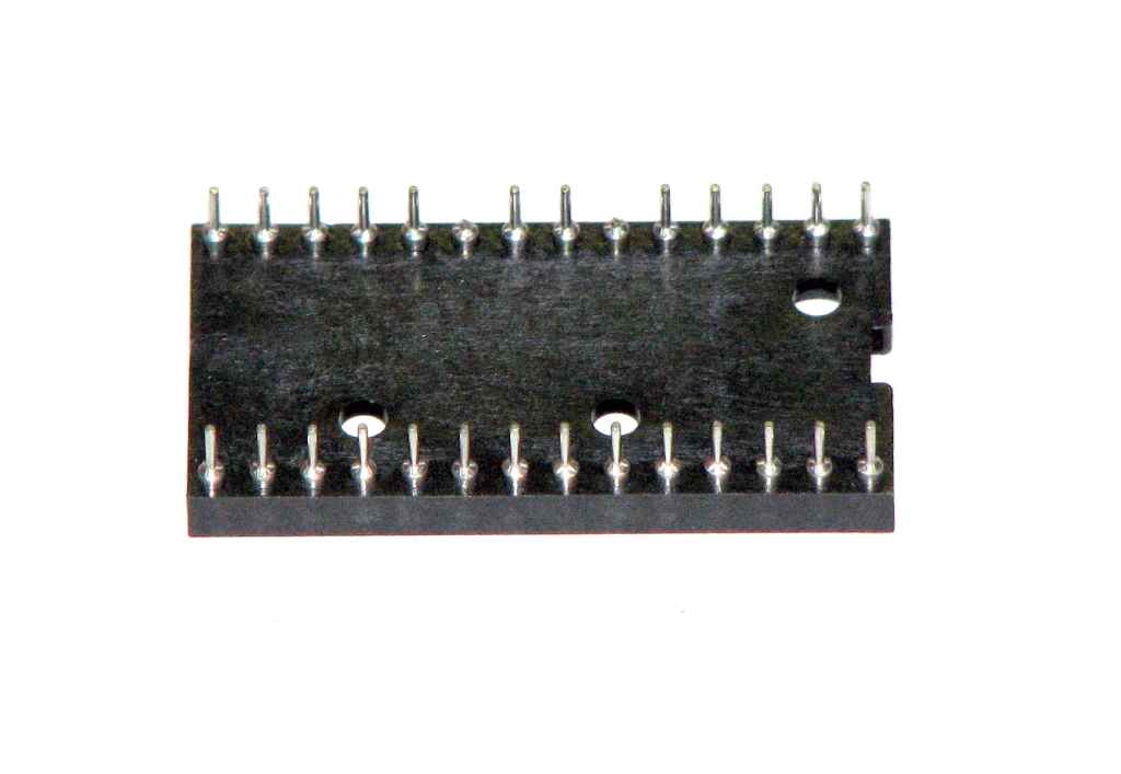 |
Step 2: On the 28-pin socket, cut pins 20 & 23 down to about 1.5mm, where the thin socket leg gets fatter at the base. |
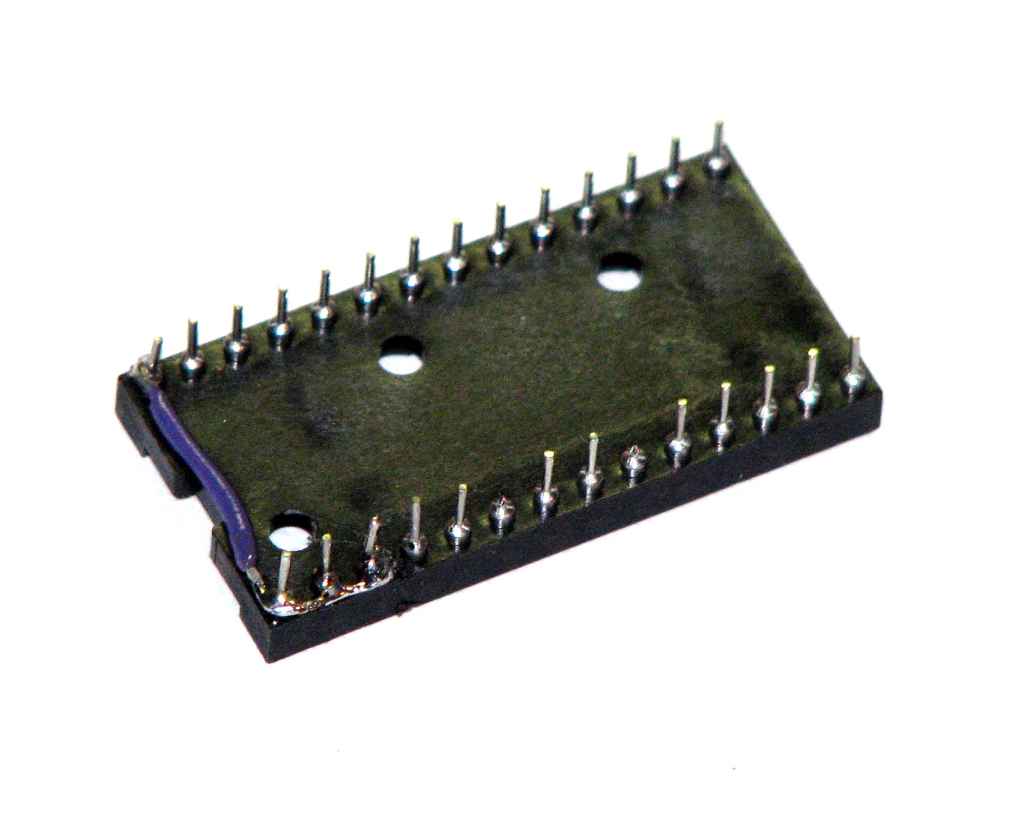 |
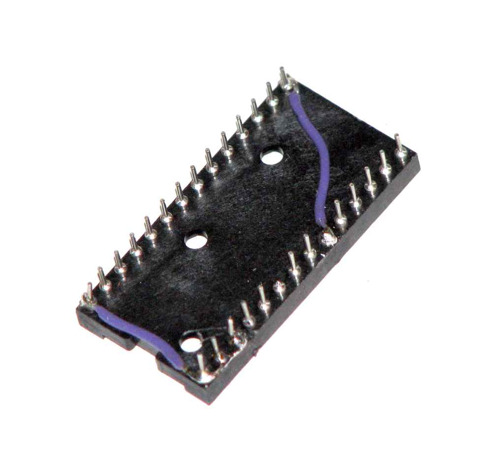
Step 3: On the 28-pin socket, solder a jumper wire from pin 1 to three sequential pins 28-27-26. Note to leave the wire shielded between pin 1 and 28, but unshielded from 28 to 26. |
 |
Step 4: On the 28-pin socket, solder a jumper from pin 14 to 20 (one of the cut pins). |
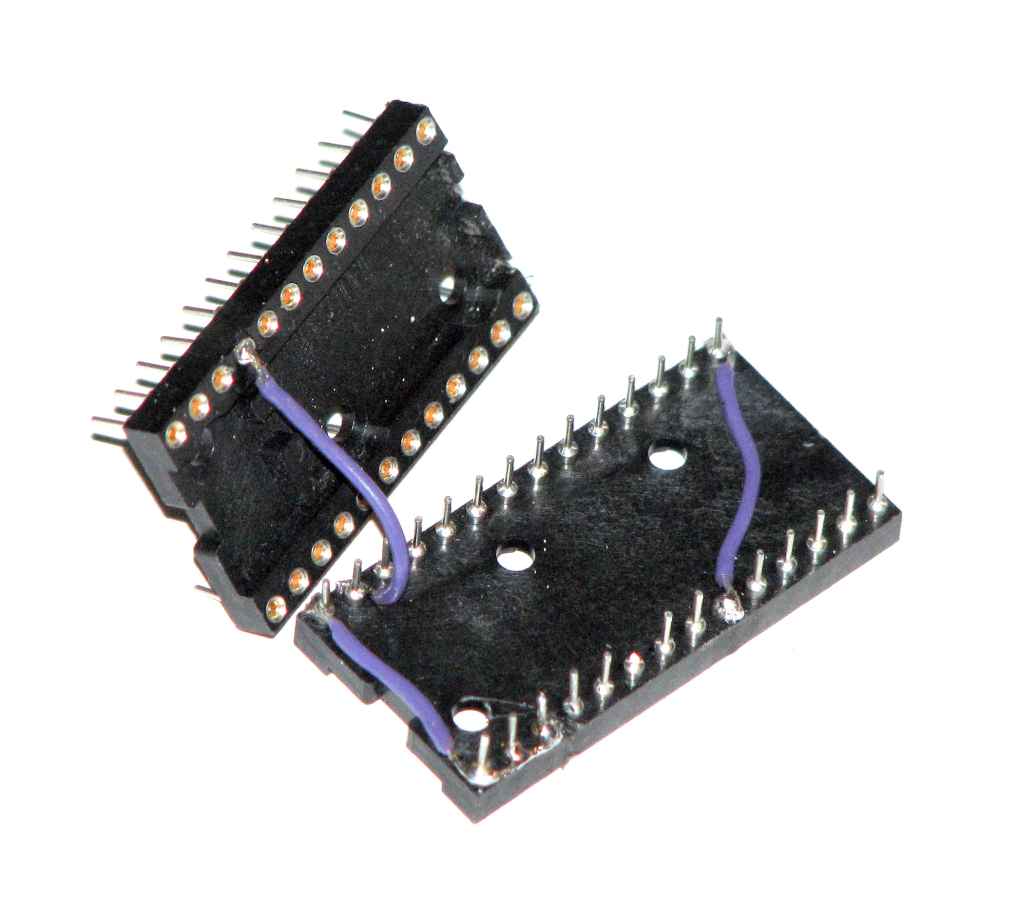 |
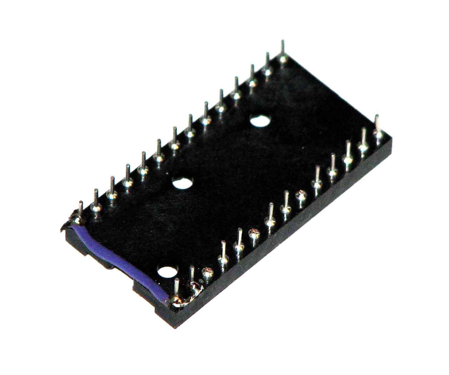
Step 5: On the 28-pin socket, solder a wire to pin 2. Cut it at about 1" (2.5cm) and solder it into hole 21 on the 24-pin socket. |
 |
Step 6: On the 28-pin socket, solder a wire to pin 23 (another cut pin). Cut it at about 1" (2.5cm) and solder it into hole 18 on the 24 pin socket. |
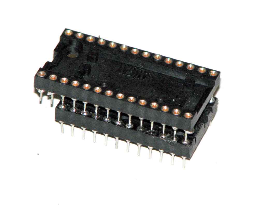 |
Step 7: Put the sockets above each other, matching pin 14 on the 28-pin socket with pin 12 on the 24-pin socket (the right egdes of the sockets are aligned, assuming the left edge of the sockets have the pin 1 notch). Don't squish the sockets together as the wires soldered into the holes on the 24-pin socket will touch the pins that were cut on the 28-pin socket. All full-length pins from the 28-pin socket must be soldered to the holes on the 24-pin sockets. Start by soldering opposite corners, then solder the rest. |
Socket Adapter Pinout Chart
24-pin socket |
28-pin Socket |
|---|---|
1 (A7)
|
3 (A7)
|
2 (A6)
|
4 (A6)
|
3 (A5)
|
5 (A5)
|
4 (A4)
|
6 (A4)
|
5 (A3)
|
7 (A3)
|
6 (A2) |
8 (A2)
|
7 (A1) |
9 (A1) |
8 (A0) |
10 (A0) |
9 (D0) |
11 (D0) |
10 (D1) |
12 (D1) |
| 11 (D2) | 13 (D2) |
| 12 (GND) | 14 (GND), 20 (CE) |
| 13 (D3) | 15 (D3) |
| 14 (D4) | 16 (D4) |
| 15 (D5) | 17 (D5) |
| 16 (D6) | 18 (D6) |
| 17 (D7) | 19 (D7) |
| 18 (A11) | 23 (A11) |
| 19 (A10) | 21 (A10) |
| 20 (CE) | 22 (OE) |
| 21 (A12) | 2 (A12) |
| 22 (A9) | 24 (A9) |
| 23 (A8) | 25 (A8) |
| 24 (Vcc) | 26 (N/C), 27 (PGM), 28 (Vcc), 1 (Vpp) |
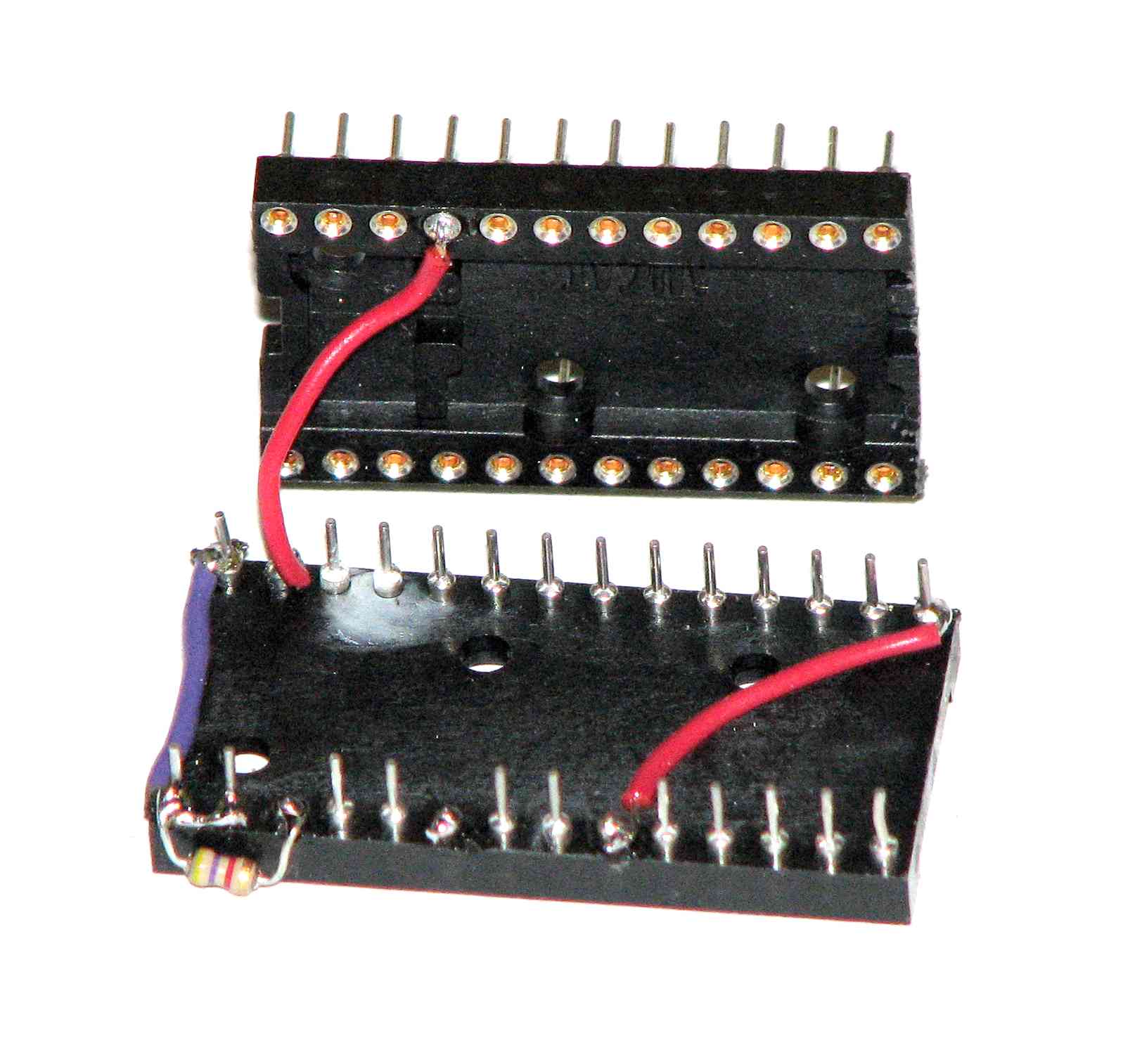
Building a 28-24 Pin ROM adapter for 27128 EPROMs for the original C64's and 1541's.
This socket adapter provides the ability to have two ROM images (i.e. two KERNALS) which can be switched when needed. This adapter is very similar to the 2764 adapter above, but one extra address line must be dealt with.
|
Step 1: Obtain a 28 pin and 24 pin precision socket. These have the round pins (not flat) and are more expensive than standard chip sockets. The 28 pin will go on the top and the 24 pin will be on the bottom when completed. |
 |
Step 2: On the 28-pin socket, cut pins 20, 23 & 26 down to about 1.5mm, where the thin socket leg gets fatter at the base. Pin 26 is the extra pin difference from the 2764 socket above as it is the extra address line. |
 |
Step 3: On the 28-pin socket, solder a jumper wire from pin 1 to two sequential pins 28-27. Note to leave the wire shielded between pin 1 and 28, but unshielded from 28 to 27. |
 |
Step 4: On the 28-pin socket, solder a jumper from pin 14 to 20 (a short pin). |
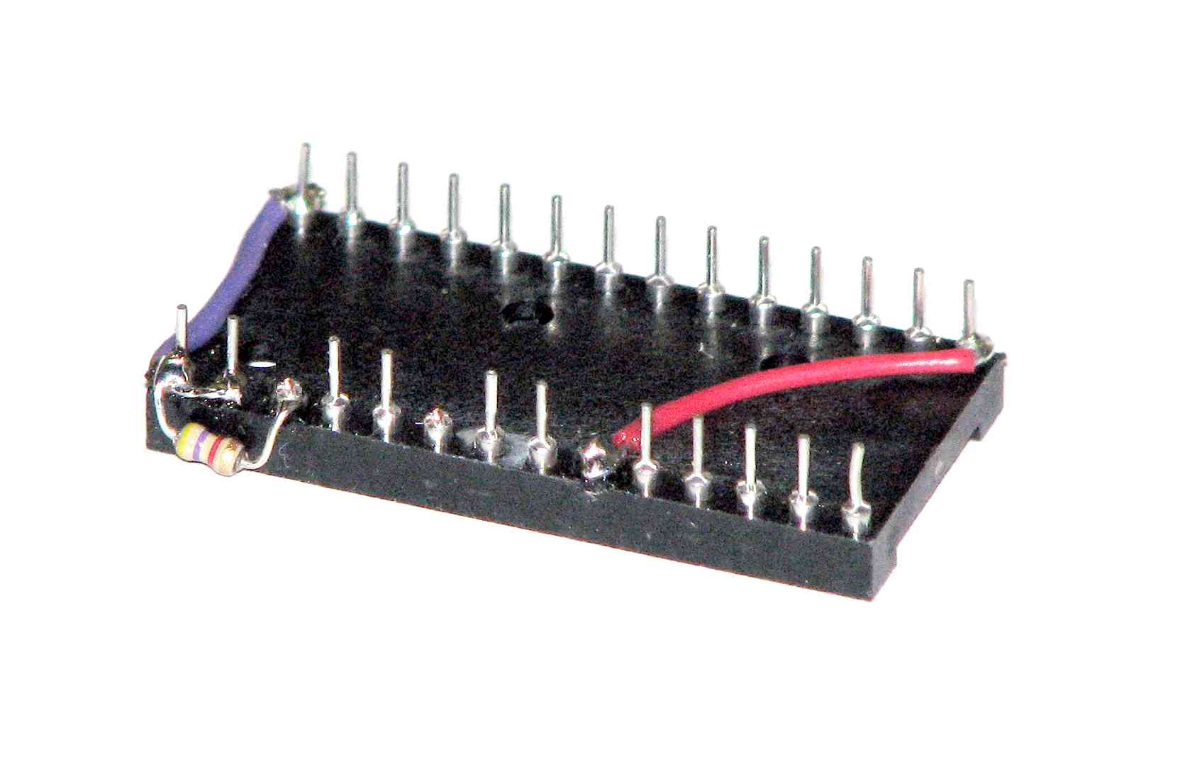 |
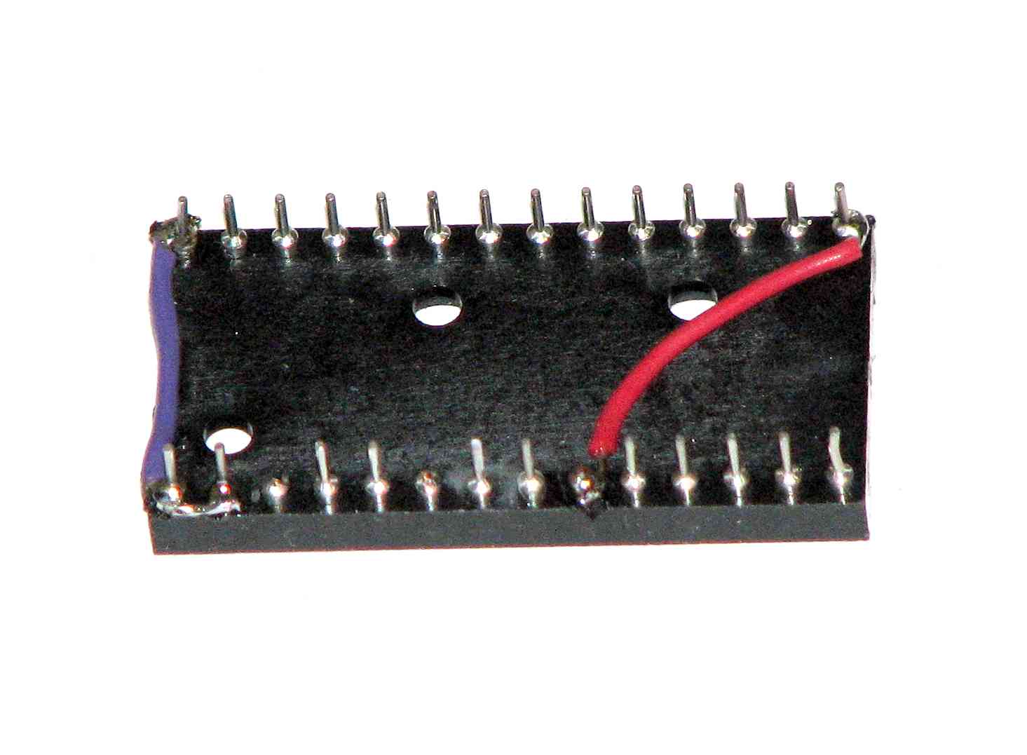
Step 5: Solder a 4.7k resistor between pins 28 and 26 on the 28 pin socket. I used a 1/8 watt resistor as it is much smaller and hence fits well against the side of the socket. Pin 26 is the high (extra) address line which will be used to switch between the two ROM images. (I guess I could have placed the resistor on the bottom of the socket instead of on the side as it would be between the two sockets when the adapter was completed and hence out of the way. This method should allow you to use the slightly larger 1/4 watt resistor instead.) |
 |
Step 6: On the 28-pin socket, solder a wire to pin 2. Cut it at about 1" (2.5cm) and solder it into hole 21 on the 24-pin socket. |
 |
Step 7: On the 28-pin socket, solder a wire to pin 23. Cut it at about 1" (2.5cm) and solder it into hole 18 on the 24 pin socket. |
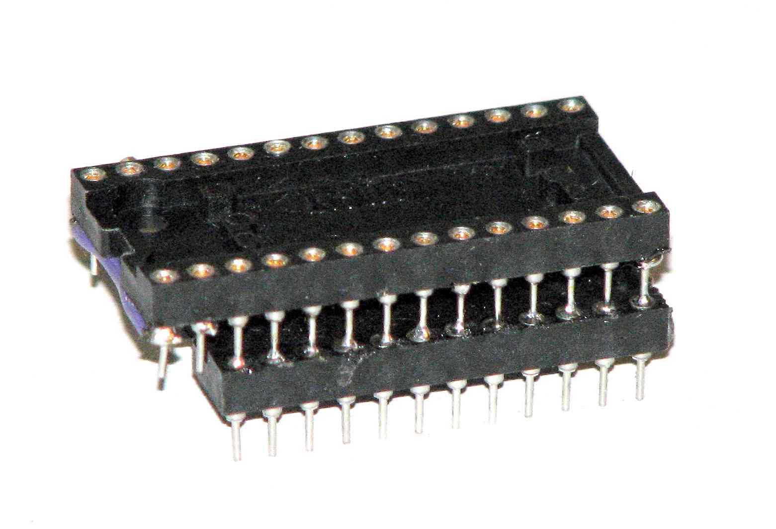 |
Step 8: Put the sockets above each other, matching pin 14 on the 28-pin socket with pin 12 on the 24-pin socket (the right egdes of the sockets are aligned, assuming the left edge of the sockets have the pin 1 notch). Don't squish the sockets together as the wires soldered into the holes on the 24-pin socket will touch the pins that were cut on the 28-pin socket. Instead, the pin should just start going into the hole beneath it, then solder it in. Start by soldering opposite corners, then solder the rest. All full-length pins from the 28-pin socket must be soldered to the holes on the 24-pin sockets. |
| Step 9: Solder a jumper between pin 24 (from the solder cup) on the 24-pin socket to pin 27 on the 28 pin socket. It's easy as they are right next to each other. This jumper provides power to the 28-pin socket. | |
| Step 10: Solder long wires to pin 26 and pin 14 on the 28 pin socket. These will be soldered to a SPST switch which is used to switch between the two ROM images. |
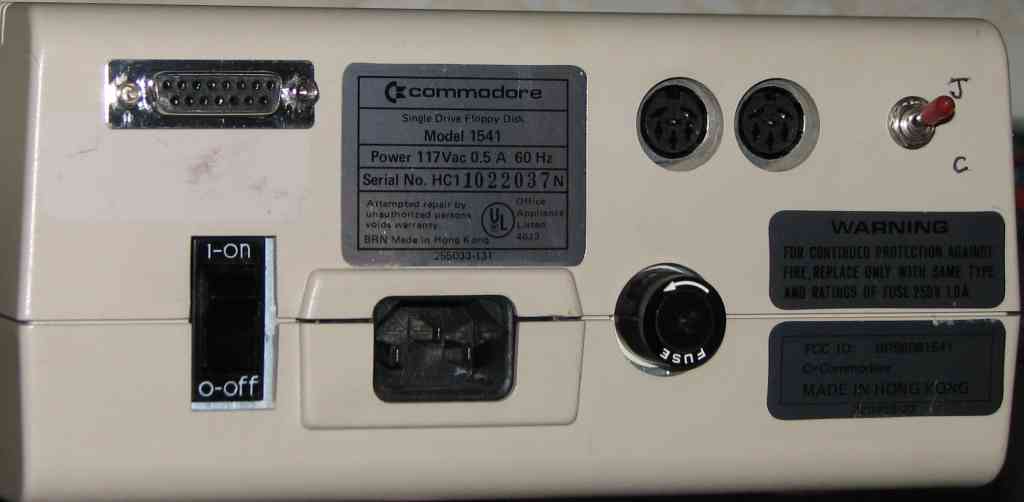
Finished & Installed Socket Adapter in the 1541

|
The socket for the 27128 installed in a 1541 long-board, with two different Kernals burned, and the switch mounted through the back case. |
 |
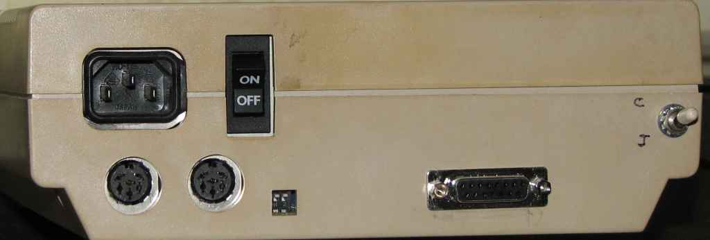
The rear of the 1541, with both the Kernal switch and the parallel port add-on. |
Socket Adapter Pinout Chart
24-pin socket |
28-pin Socket |
|---|---|
1 (A7)
|
3 (A7)
|
2 (A6)
|
4 (A6)
|
3 (A5)
|
5 (A5)
|
4 (A4)
|
6 (A4)
|
5 (A3)
|
7 (A3)
|
6 (A2) |
8 (A2)
|
7 (A1) |
9 (A1) |
8 (A0) |
10 (A0) |
9 (D0) |
11 (D0) |
10 (D1) |
12 (D1) |
| 11 (D2) | 13 (D2) |
| 12 (GND) | 14 (GND), 20 (CE) |
| 13 (D3) | 15 (D3) |
| 14 (D4) | 16 (D4) |
| 15 (D5) | 17 (D5) |
| 16 (D6) | 18 (D6) |
| 17 (D7) | 19 (D7) |
| 18 (A11) | 23 (A11) |
| 19 (A10) | 21 (A10) |
| 20 (CE) | 22 (OE) |
| 21 (A12) | 2 (A12) |
| 22 (A9) | 24 (A9) |
| 23 (A8) | 25 (A8) |
| 24 (Vcc) | 27 (PGM), 28 (Vcc), 1 (Vpp) |
| 26 --\/\/\/-- 28 (resistor) | |
| 14 --/ --- 26 (switch) |
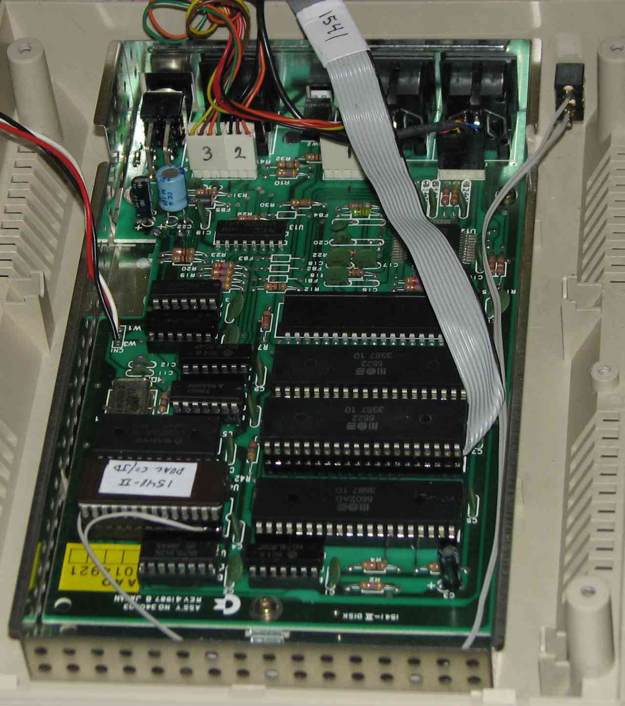
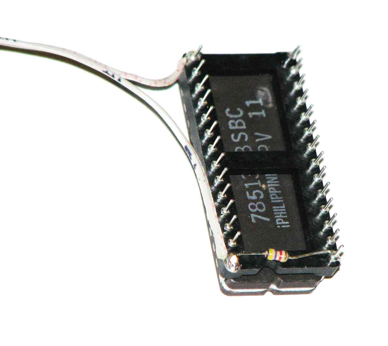
Building a 27128 to 27256 Adapter Socket for the 1541-II and 1541C
This socket adapter allows you to have 2 Kernals installed, with a switch to change between them. This is a simpler project than the 1541 because it only needs one 28-pin socket instead of stacking them. Also, you only need to cut one pin, solder a 4.7K resistor between pin 27 and 28 and wire in an SPST switch between pin 27 and pin 14..
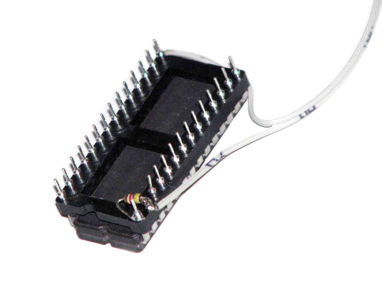 |
This is the adapter socket for putting a 27256 into the space for a 27128, like the 1541-II and 1541C, or even the C64C. Cut pin 27 (A14) short, and solder a 4.7K resistor between pins 27 and 28. Then solder a switch to pin 27 and pin 14 (GND) to allow switching between the two Kernals. |
Finished & Installed Socket Adapter in a 1541C
 |
The socket adapter for the 27256 installed in the 1541C, with two different Kernals burned, and the switch mounted through the back case. |
 |
The rear of the 1541c, with both the Kernal switch and the parallel port add-on. |
Finished & Installed Socket Adapter in a 1541-II
 |
The socket adapter for the 27256 installed in the 1541-II, with two different Kernals burned, and the switch mounted through the back case. |
 |
The rear of the 1541-II, with both the Kernal switch and the parallel port add-on. |
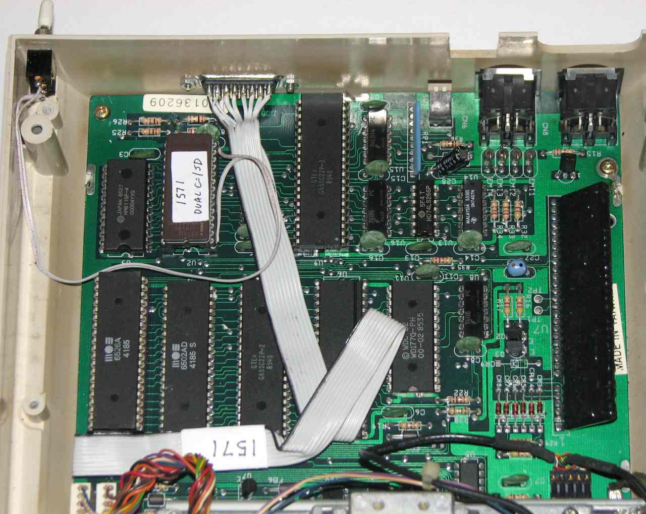
Building a 27256 to 27512 Socket Adapter for 1571
This adapter socket lets you install two Kernals in your 1571, with a switch to change between them. This is an easy project as it only involves one 28-pin socket, cut pin 1, solder a 4.7K resistor and wire in an SPST switch to change between the Kernals.
 |
This is the adapter socket for putting a 27512 into the space for a 27256 in the 1571. Cut pin 1 (A15) short, and solder a 4.7K resistor between pins 1 and 28. Then solder a switch to pin 1 and pin 14 (GND) to allow switching between the two Kernals. |
Finished & Installed Socket Adapter in a 1571
 |
The socket adapter for the 27512 installed in the 1571, with two different Kernals burned, and the switch mounted through the back case. There's very little space along with back of the 1571, so this is about the best spot for it. Also, top of the Kernal EPROM/adapter socket will touch the power supply, causing it to stand off its mounts a bit. |
 |
The rear of the 1571 with both the Kernal switch and the parallel port add-on. |
Email the author: Peter Schepers | Last updated: July 13, 2009